
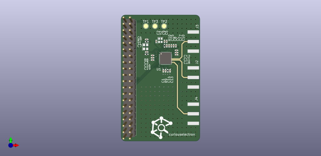
In a quest to measure the input impedance of the CC1200’s LNA in the 2m amatuer radio band, I created a basic development board for the CC1200. The data lines were broken out to a raspberry-pi header, and the RF lines were routed out to edge mount SMA connectors via 50Ohm microstrip. The stackup was JLC2313.
This design had a number of issues.
- JLCPCB offers a calculator which accounts the soldermask. I didn’t use this tool and instead used KiCad’s built-in calculator which doesn’t account for soldermask. To eliminate this variable, I removed solder mask from the RF traces. This is a common practice, but in the future I should make sure to keep soldermask within the courtyard of the CC1200.
- I designed the microstrip to use the 7XXX stackup offered by JLCPCB and not 2313 :D, opps.
- The PA and LNA traces are different lengths! This means in order to de-embedded the measurements, I need to calculate the phase-delay for each length (assuming the microstrip is actually 50Ohms…it wasn’t) or perform additional measurements to de-embedded.
- The SMA footprint is poorly matched, but to be frank – I wasn’t completely sure of this at this time.
In light of all these issues, I decided to run back to basics and create a basic coupon based on the JLC2313 stackup using the JLCPCB calculator. The coupon was designed to used as a SOL cal standard for de-embedding a 20mm microstrip trace. A 40mm microstrip through connection was also added to quickly confirm the performance of the stackup.
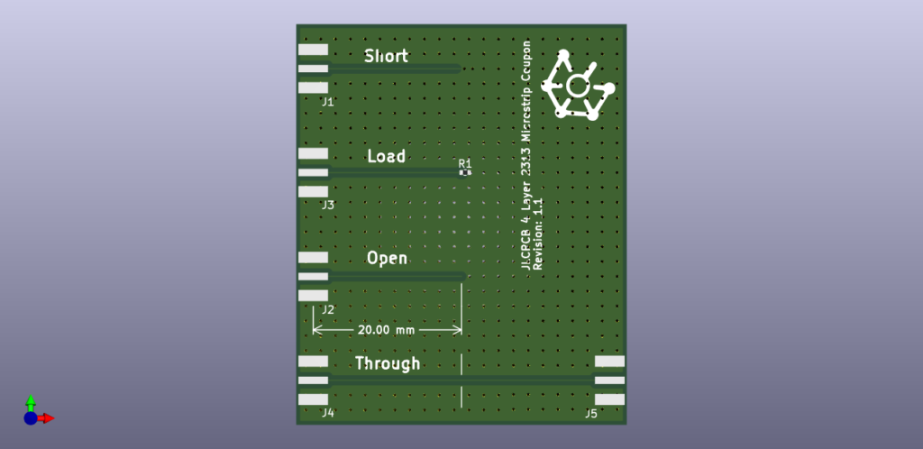
Lastly, after reading a few papers on proper signal launch and reviewing data from the defunked CC1200 development board, I decided to order two versions of the coupon with different versions of the SMA footprint. Both are optimized to have the smallest possible center pin pad, but version v1.0 has ground underneath the center pin, and version v1.1 has a keepout for all copper under the center pin.
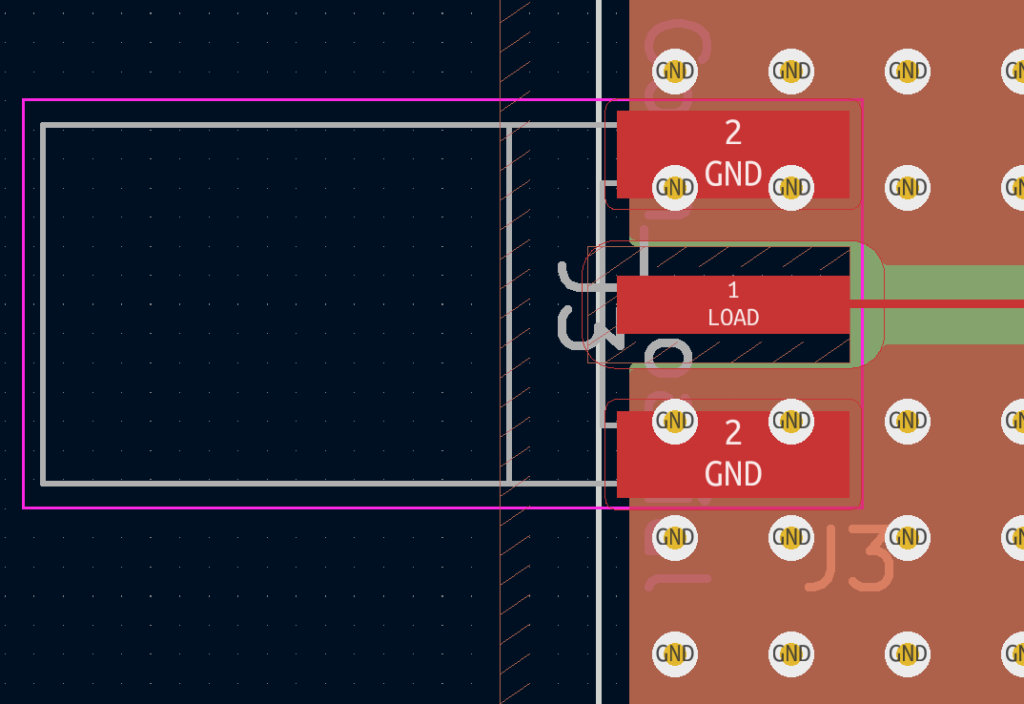
Removal of copper under the center pin was critical to achieving an excellent match. The data below was collected using the NanoVNA V2.4 using the curiousmeasurements python package. 
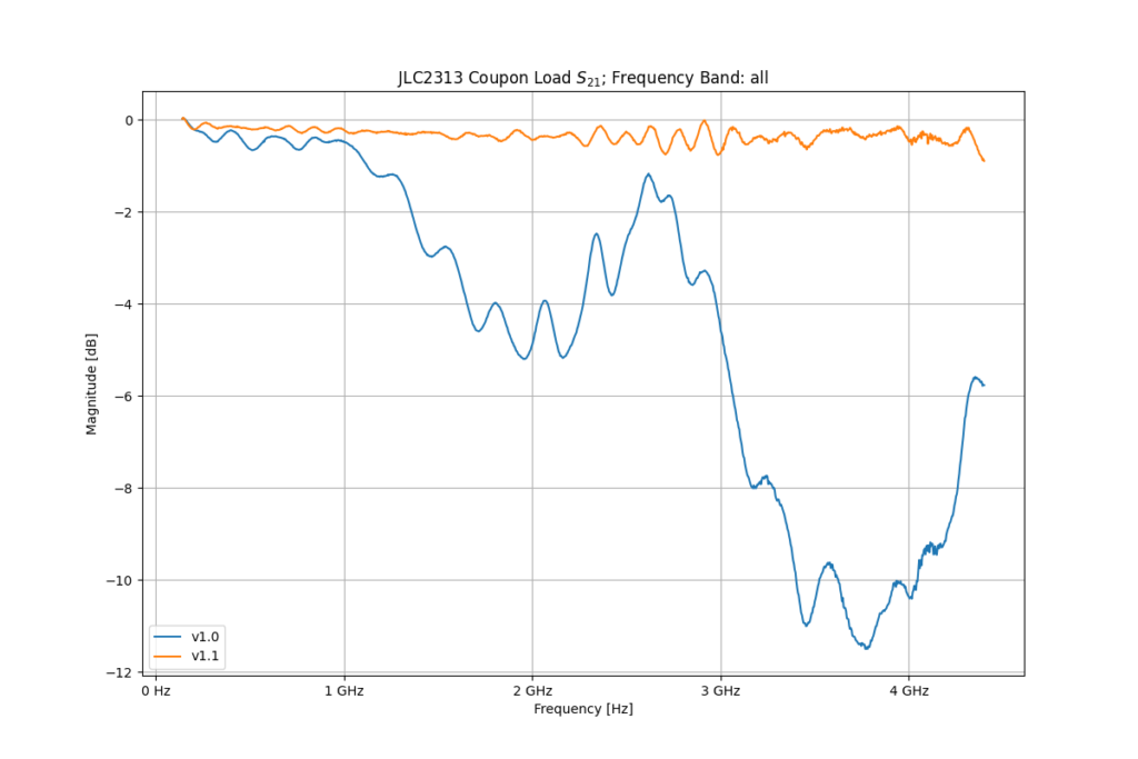
Version v1.0’s match is unusable above 1GHz, while v1.1 has a return loss <-10dB all the way to 4.4GHz. Not bad for some no-name Amazon SMA connectors…
The same continues for transfer response. The performance is excellent for v1.1. I was quite surprised how much such a small change drastically improved performance.